The introduction of digital signal processing in sound recording and reproduction systems imposes stringent requirements on the performance of digital-ta-analogue converters (DACs). Many of these systems demand converters with up to 16-bit resolution to obtain sufficiently high signal-to-noise ratio and good linearity.
The Philips TDA1540 is the first monolithic bipolar 14-bit DAC with a signal-to-noise ratio of 85 dB (typ) for audio signals, sampled at 44 kHz. It uses a new method of current division, called dynamic element matching, to long-term stability. Dynamic element matching combines passive division with a time division concept which eliminates resistor trimming
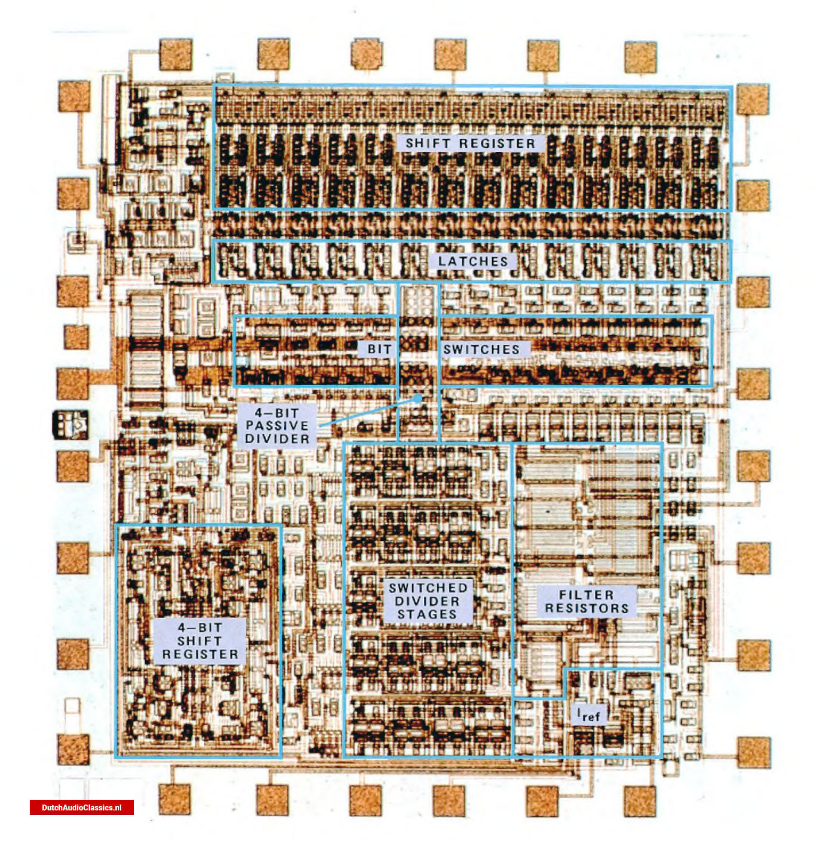
![Philips TDA1540 - Layout of the 3.0 x 3.4mm Philips TDA1540 chip]() Layout of the 3.0 x 3.4mm Philips TDA1540 chip
Layout of the 3.0 x 3.4mm Philips TDA1540 chip
In addition, the TDA1540 features:
- on-chip serial-to-parallcl shift register and data latches
- on-chip current reference
- inherent monotonicity from —25 to +70 °C
- TTL compatible input
- serial data input (offset binary) which reduces feed through and correlated noise
- improved bit switching no deglitching circuit required
Tabic 1 gives further data on the Philips TDA1540
| Table 1: Philips TDA1540 data |
| Resolution: |
14 bits |
| Signal-to-noise ratio* (typ.): |
85dB |
| Linearity (typ.): |
+/- 1/4 LSB at Tamb = 25°C |
|
+/- 1/2 LSB -20°C < Tamb < +70°C |
| Full-scale current (typ.): |
4mA |
| Settling time to +1/2 LSB (for a full-scale charge): |
Typ. 1μs |
| Maximum input bit rate: |
12 Mbit/s |
| Power dissipation: |
350 mW |
| Supply voltages: |
+5 V, —5 V and -17 V |
| Encapsulation: |
28-pin ceramic DIL |
| * measured between 31,5 Hz and 20 kHz at a sampling frequency of 44 kHz. |
| Table 2: Matching tolerance of different types of resistor |
| Fabrication process: |
Matching tolerance |
|
σ(%) |
mean(%) |
|
10 μm |
40 μm |
10 μm |
40 μm |
| Diffusion |
0.44 |
0.23 |
-0.1 |
0.07 |
| Thin-film |
0.24 |
0.11 |
-0.1 |
-0.06 |
| Ion implantation |
0.34 |
0.12 |
-0.04 |
-0.05 |
| Resistor linewidth 10 μm and 40 μm |
Standard Digital-to-analogue conversion techniques
Monolithic DACs widely use an R-2R fesistive ladder network with multiple-emitter terminating transistors to generate binary-weighted currents. These currents are switched by digitally-controlled switches (bit switches) to a summing point; thereby digital-to-analogue signal conversion is performed. Figure 1 shows a DAC of this type.
There are two problems in the design of an R-2R DAC: the weighting accuracy of the binary currents which is set by the tolerance of the resistors and transistors, and the switching of the accurately weighted binary currents without glitches which determines the dynamic performance. Regarding the problem of accuracy, Table 2 shows that it is straightforward to integrate DACs having up to 10 bits; a 1 0 bit converter requires a 512:1 current division, i.e. requires resistor tolerance better than 0.05%. Twelve-bit converters usually need laser trimming of thin-film resistors, or trimming of the binary-weighted currents using Zener zapping to achieve 12-bit accuracy.
![Philips TDA1540 - 3-bit binary-weighted R-2R digital-to-analogue converter]() Figure l - 3-bit binary-weighted R-2R digital-to-analogue converter
Figure l - 3-bit binary-weighted R-2R digital-to-analogue converter
It is questionable how successfully trimming can be applied to 14 or 16-bit converters. Mounting the chip after trimming can change the resistances; trimming after mounting can be expensive. Long-term stability may be a problem too. Furthermore, the cost of laser trimming in large-volume production can be significant.
In the TDA1540 trimming has been eliminated by dynamic element matching.
Dynamic element matching
Basic current divider
Figure 2(a) shows the block diagram of the divider. It consists of a passive current divider and a set of switches driven at a frequency f by a clock pulse generator.
The input current 2I is divided into two nearly equal parts: I1 = 1 + Δl and I2 = I - Δl. Then, I1 and I2 are interchanged with respect to the output terminals 3 and 4 for equal times by means of the switches. The average current at each output terminal is then exactly equal and has a value I, see Fig.2(b).
By cascading divider stages an accurate binary-weighted current network is formed. However, in a practical circuit, each stage requires a minimum supply voltage of ≈2V. This leads to an impractically large supply voltage for a 14-bit current network. Therefore, an improved divider is used which gives more weighted currents in one current interchange.
![Philips TDA1540]() Figure 2
Figure 2
Improved divider
In the improved divider, a current 4I is divided into four nearly equal parts: I + Δ1I, I + Δ2I, I + Δ3I and I + Δ4I, see Fig.3(a). Note that Δ1 + Δ2 + Δ3 + Δ4 = 0.
![Philips TDA1540 - (a) Improved current divider. (b) Output currents I1, I2 and I3]() Figure 3 - (a) Improved current divider. (b) Output currents I1, I2 and I3
Figure 3 - (a) Improved current divider. (b) Output currents I1, I2 and I3
These currents are fed into a switching network which interchanges all the currents with respect to the output terminals for equal times. The switches are controlled by signals from a 4-bit shift register.
At the output of the switching network, two currents are combined; thus, the output currents have average values of 2I, I and I, Fig.3(b). All currents have a ripple of frequency f/4 (the time for one complete interchange of the four currents being 4/f). Timing errors in the current switching have the same effect on accuracy as for the basic divider
Figure 4 shows the circuit diagram of a practical current divider. Transistors TR1, TR2, TR3 and TR4, with the resistors R divide the current 41 into four nearly equal currents. These currents are fed into the switching network which consists of Darlington transistor switches to minimise base current loss. Two currents are summed directly giving an output current of 2I (av.). A 4-bit shift register controls the transistor switches which for accurate current division must have high current gain.
![Philips TDA1540 - Circuit diagram of the practical current divider]() Figure 4 - Circuit diagram of the practical current divider
Figure 4 - Circuit diagram of the practical current divider
Binary-weighted current network
By cascading divider stages, a binary-weighted current network is formed, see Fig.5. In the first stage the onchip reference current source licf and a current amplifier form an accurate current mirror. The reference current is used as the most significant bit current, which eliminates filtering.
To obtain 14-bit accuracy, a choice can be made between the number of switched and unswitched current dividers. The minimum supply voltage decreases as the number of unswitched dividers increases. However, the number of unswitched dividers is limited by circuit yield. Five switched dividers followed by a 4-bit passive divider using emitter scaling represents the best compromise between supply voltage and circuit yield.
Filters and BIT switches
Figure 6 shows how the output currents of a switched divider stage are filtered and switched to the output. R1C1 and R2C2 form first-order filters (the capacitors are connected externally). Darlington transistors TR3, TR4 and TR5, TR6 isolate the filters from the switching of the binary-weighted currents to the output (bit switching). Bit switching is performed with a diodetransistor configuration TR1. D1 and TR2, D2, enabling fast and accurate switching with no loss of base currents.
![Philips TDA1540 - Binary-weighted current network]() Figure 5 - Binary-weighted current network
Figure 5 - Binary-weighted current network
![Philips TDA1540 - Filtering and switching the binary-weighted currents to the output]() Figure 6 - Filtering and switching the binary-weighted currents to the output
Figure 6 - Filtering and switching the binary-weighted currents to the output
Individual filtering of bit currents minimises the noise of the TDA1540 output current, and makes the conversion tinre solely dependent upon the speed of the bit switches.
Complete 14-BIT DAC
Figure 7 is the block diagram of the complete DAC. It shows the 14-bit binary-weighted current network, the reference current source, individual bit-current filters and the bit switches. The shift register that controls the Darlington transistor switches is at the bottom of the figure.
Figure 8 shows how to obtain a voltage output using the TDA1540 with an operational amplifier.
Figure 9 shows the input data format D, and the corresponding timing signals CP (clock input) and LE (latch enable).
![Philips TDA1540 - Block diagram]() Figure 7 - Block diagram of the Philips TDA1540
Figure 7 - Block diagram of the Philips TDA1540
![Philips TDA1540 - Circuit diagram of a voltage-output digital-to-analogue converter using the Philips TDA1540]() Figure 8 - Circuit diagram of a voltage-output digital-to-analogue converter using the Philips TDA1540
Figure 8 - Circuit diagram of a voltage-output digital-to-analogue converter using the Philips TDA1540
![Philips TDA1540 - timing diagram]() Figure 9 - Philips TDA1540 timing diagram
Figure 9 - Philips TDA1540 timing diagram
![Philips TDA1540 - Non-linearity of the Philips TDA1540 as a function of temperature]() Figure 10 - Non-linearity of the Philips TDA1540 as a function of temperature
Figure 10 - Non-linearity of the Philips TDA1540 as a function of temperature
![Philips TDA1540 - Arrangement for measuring dynamic performance]() Figure 11 - Arrangement for measuring dynamic performance
Figure 11 - Arrangement for measuring dynamic performance
Performance
Linearity
A DAC is monotonic, if the non-linearity is less than +/- 1/2 LSB. Figure 10 shows that the non-linearity of the TDA1540 is typically less than 1/2 LSB (3 x 10 -5) over the temperature range —20 to +70 °C.
Dynamic performance
Figure 11 shows the arrangement used to measure dynamic performance. A digital sine wave source produces 14-bit words which are- latched at 44 kHz. The outputs of the latches drive directly the bit switches of the converter. A high-speed operational amplifier with feedback resistor R converts the output current of the converter into a voltage suitable for examination by spectrum analyser and oscilloscope, or distortion analyser.
Figure 12 shows the results of spectrum analysis. For sine waves of 600 Hz, 5.5 kHz and 18 kHz, distortion is about —90dB with respect to the maximum sine wave output. Note, -90dB is the limit of resolution of the spectrum analyser
Figure 13 shows oscillograms of the filtered and unfiltered output signals. The low-pass filter introduces a delay in the output signal.
![Philips TDA1540 - Distortion of an output sinewave of frequency 600 Hz, 5.5 kHz and 18 kHz, respectively. Vertical scale 10 dB/div., horizontal scale 2 kHz/div. Bandwidth 30 Hz]() Figure 12 - Distortion of an output sinewave of frequency 600 Hz, 5.5 kHz and 18 kHz, respectively. Vertical scale 10 dB/div., horizontal scale 2 kHz/div. Bandwidth 30 Hz
Figure 12 - Distortion of an output sinewave of frequency 600 Hz, 5.5 kHz and 18 kHz, respectively. Vertical scale 10 dB/div., horizontal scale 2 kHz/div. Bandwidth 30 Hz
![Philips TDA1540 - Filtered and unfiltered output signals: above, 1 kHz; below, 6.3 kHz. Vertical scale 0.33 volt]() Figure 13 - Filtered and unfiltered output signals: above, 1 kHz; below, 6.3 kHz. Vertical scale 0.33 volt
Figure 13 - Filtered and unfiltered output signals: above, 1 kHz; below, 6.3 kHz. Vertical scale 0.33 volt
Applications
Dynamic element matching is a simple, accurate and reliable method of current division for high-accuracy monolithic DACs; the resulting dynamic performance of the TDAl540 makes it ideal for sound reproduction and recording systems.
Its 15-bit linearity also makes it suitable for applications that do not require 14-bit resolution, but demand high linearity to improve relative accuracy. Such applications include graphic display systems, electron-beam recording and nuclear instrumentation.
The TDA1540 easily fulfills the requirements of a 12-bit DAC for telephony. For instrument manufacturers, the TDA1540 can extend present limits of performance of distortion meters, spectrum analysers, sine wave and other signal generators.
The use of over-sampling techniques with the TDA1540 further improves the S/N ratio in audio applications and simplifies output analogue filters.
Source: Philips Electronics components & applications. VOL. 2 NO. 4. August 1980
 Layout of the 3.0 x 3.4mm Philips TDA1540 chip
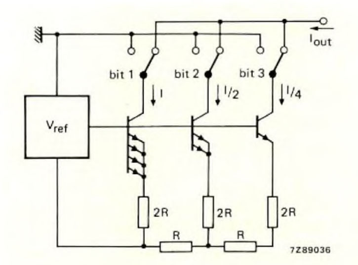 Figure l - 3-bit binary-weighted R-2R digital-to-analogue converter
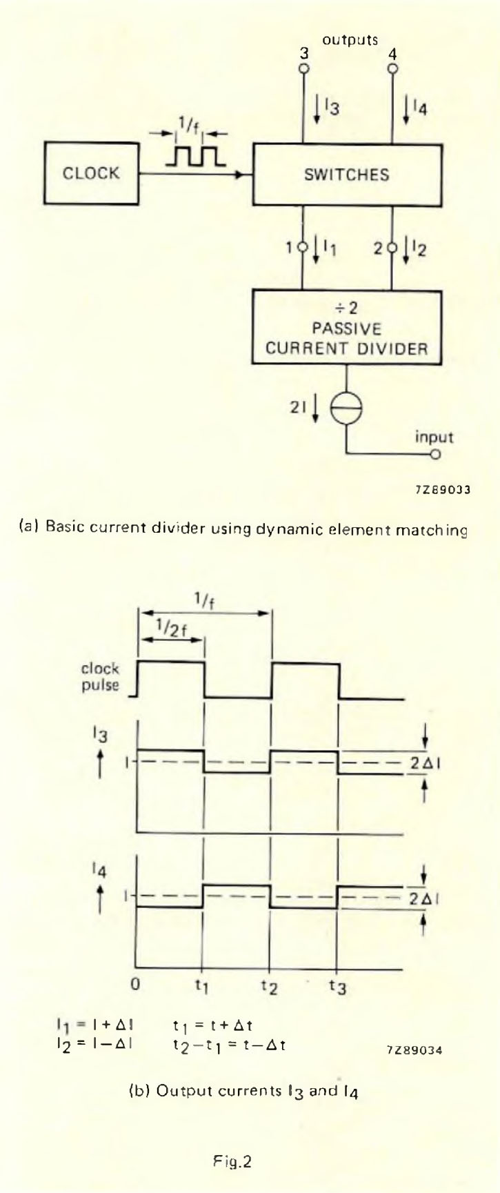 Figure 2
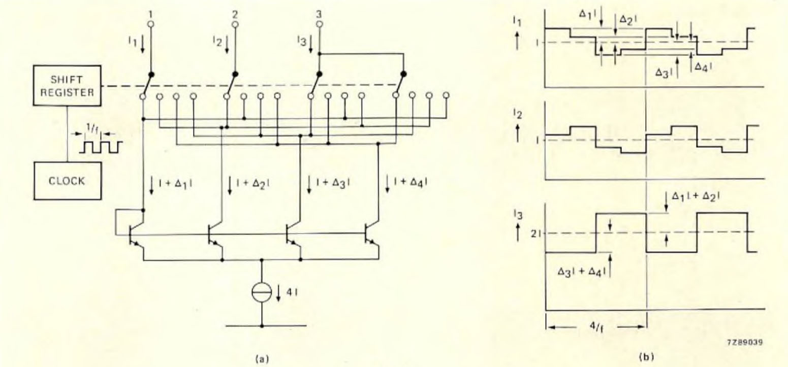 Figure 3 - (a) Improved current divider. (b) Output currents I1, I2 and I3
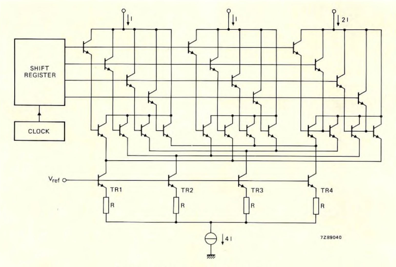 Figure 4 - Circuit diagram of the practical current divider
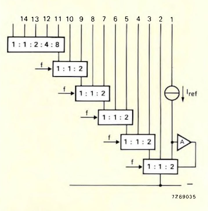 Figure 5 - Binary-weighted current network
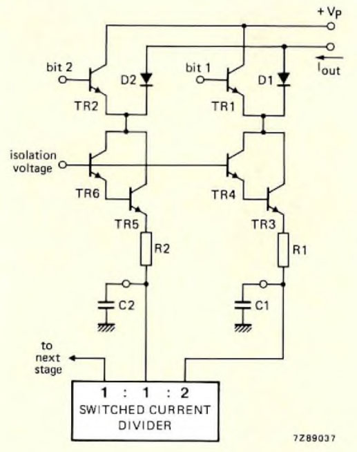 Figure 6 - Filtering and switching the binary-weighted currents to the output
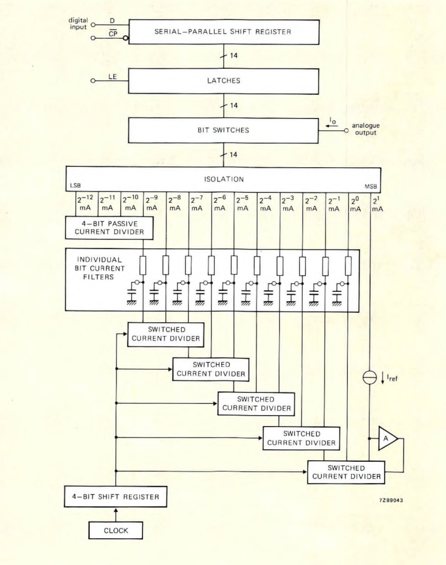 Figure 7 - Block diagram of the Philips TDA1540
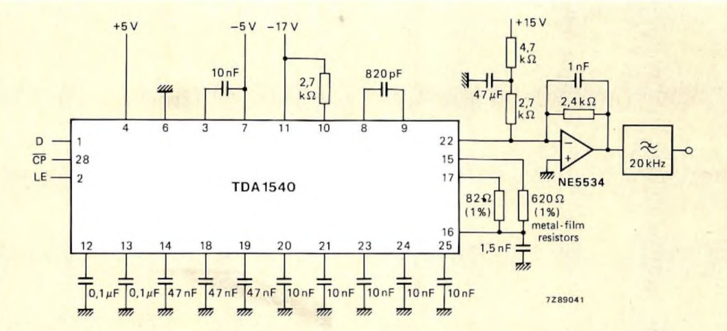 Figure 8 - Circuit diagram of a voltage-output digital-to-analogue converter using the Philips TDA1540
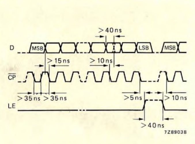 Figure 9 - Philips TDA1540 timing diagram
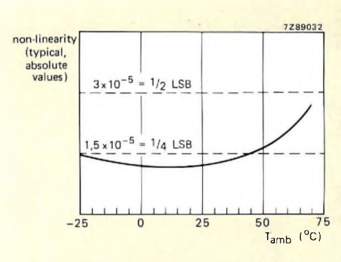 Figure 10 - Non-linearity of the Philips TDA1540 as a function of temperature
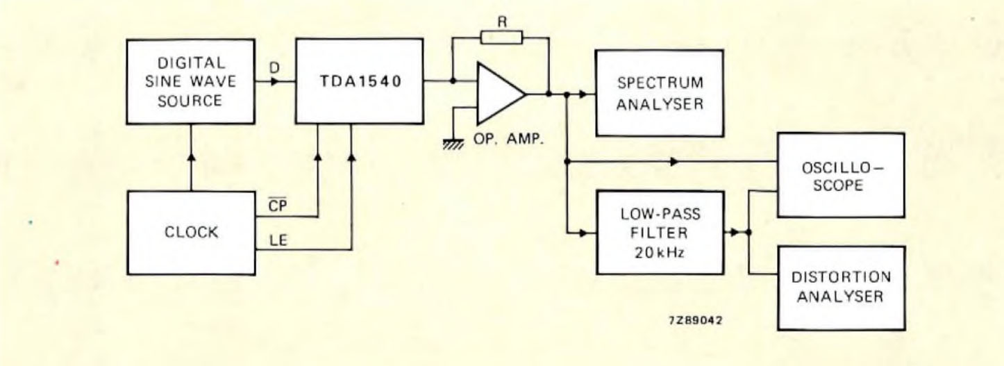 Figure 11 - Arrangement for measuring dynamic performance
 Figure 12 - Distortion of an output sinewave of frequency 600 Hz, 5.5 kHz and 18 kHz, respectively. Vertical scale 10 dB/div., horizontal scale 2 kHz/div. Bandwidth 30 Hz
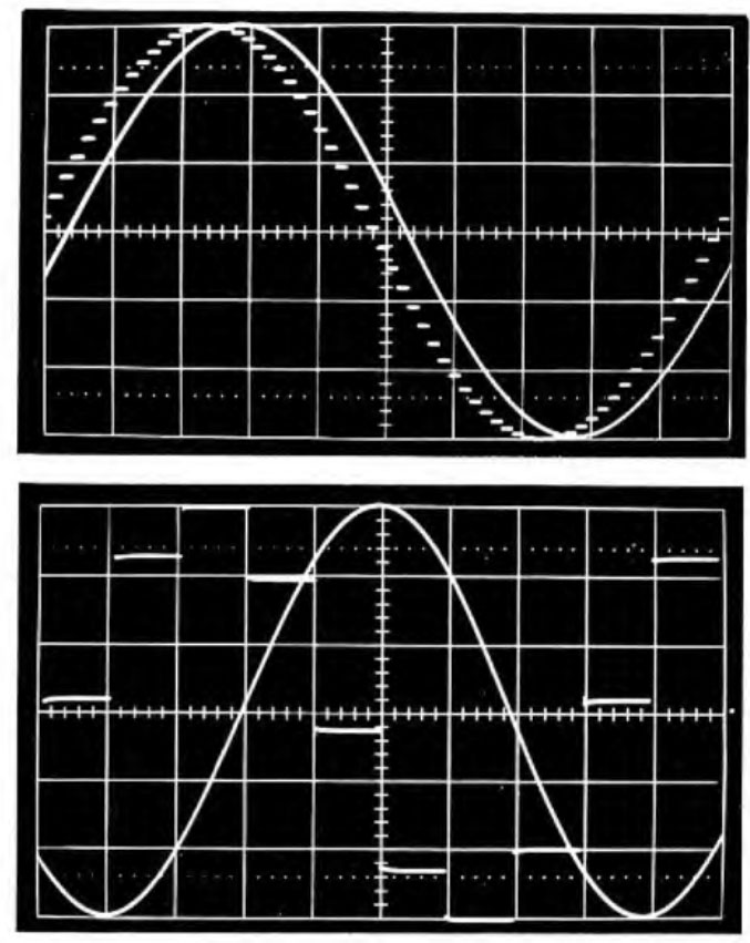 Figure 13 - Filtered and unfiltered output signals: above, 1 kHz; below, 6.3 kHz. Vertical scale 0.33 volt